Characterizing material degredation due to ion migration
As high-power, high-voltage electronics become increasingly prevalent, in electric vehicle powertrains for example, understanding the degradation of materials in close proximity to high-voltage fields is crucial. This understudied scenario and associated failure modes are quickly moving under the spotlight as industries, especially automotive, transition to electric power, which requires high voltages for fast charging and power delivery. An electric vehicle might have an 800V power train, for example. I designed a test apparatus to investigate the effects of nearby high-voltage potentials on material properties as part of a semester research and development internship at Arieca, a developer of high-performance thermal interface materials (TIMs).

Figure 1: Ion migration test apparatus.
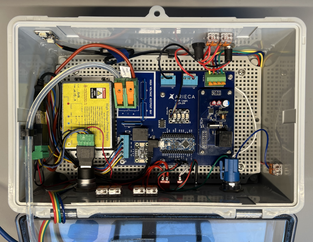
Figure 2: Internal device electronics.
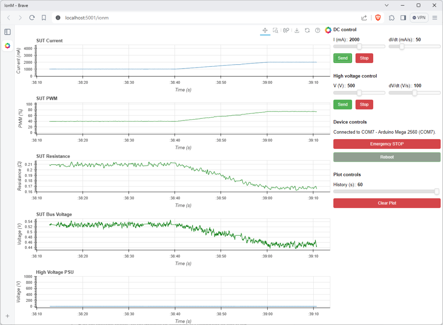
Figure 3: Real-time logging, visualization, and control interface.
We wanted to investigate the reliability and uncover failure modes of electrically or thermally conductive polymers, including liquid metal inks and Ariecaʼs TIMs, in the presence of a high-voltage electric field. The primary driver of this endeavor was to understand how ion migration in particular, initiated by the large voltage potentials, may cause material degradation. To that end, I designed and implemented a test apparatus to study the effects. This included custom printed circuit boards (PCBs) for logic, power delivery, and test samples, the device enclosure and sample holder, and a user interface. At a high level, the device consists of:
- a controllable high-voltage electrode to put sample materials near a high-voltage potential (configurable to 0-6kV);
- a controllable voltage, high-current DC power supply for biasing insulating materials or running current through conductive materials (controllable to 0-6V, 0-10A);
- a modular interface for the test electronics front-end;
- custom logic boards for interfacing with the module, controlling the high voltage, and interfacing with the controls on the enclosure;
- the device enclosure and sample holder; and
- a web-based real-time logging, visualization, and control interface.
The device firmware was developed on the Arduino platform and supports real-time sensing and command inputs. A web-based user interface was developed to visualize experimental data in real-time, log experimental data, and control the operation of the device. Figure 1 in the gallery shows the enclosure design and sample holder on top. In figure 2 you can see a birds-eye view of the assembled hardware inside. A view of the web interface can be seen in figure 3.
The first iteration of the design had some problems to address. Although most of the issues were resolved with some rework, some of the functionality was lost in the process and we wanted to ensure the design would be reliable. The second iteration was a great improvement, incorporating bug fixes along with extending capabilities. The most notable extension was the modularization of the sample under test (SUT) module. In this case, the SUT module allows for the control of a DC-DC buck converter to provide 0-6V bias on the SUT and sink up to 10A current. With the modular interface, future designs can extend capability further without requiring a complete board redesign. The second revision of the apparatus was finished toward the end of the internship, so unfortunately we were not able to conduct extensive testing prior to my departure.
We were able to capture a few interesting failures on video. Figure 4 shows a thin sample of oxidized gallium-indium liquid metal (OGaIn) with a high current density passing through it. The material quickly overheats and likely vaporizes the liquid metal, a very extreme and highly undesirable failure mode. Figure 5 shows a similar trace undergoing a more gradual degradation due to a high but more reasonable current density. Visually, the surface of the liquid metal begins to exhibit mottling, with areas of decreased reflectivity appearing first at the narrowest point of the trace where the temperature is likely highest and then propagating outward toward either end. This may be due to increased oxidation due to the elevated temperature. However, in these cases we were unable to investigate the phenomena further due to time constraints.
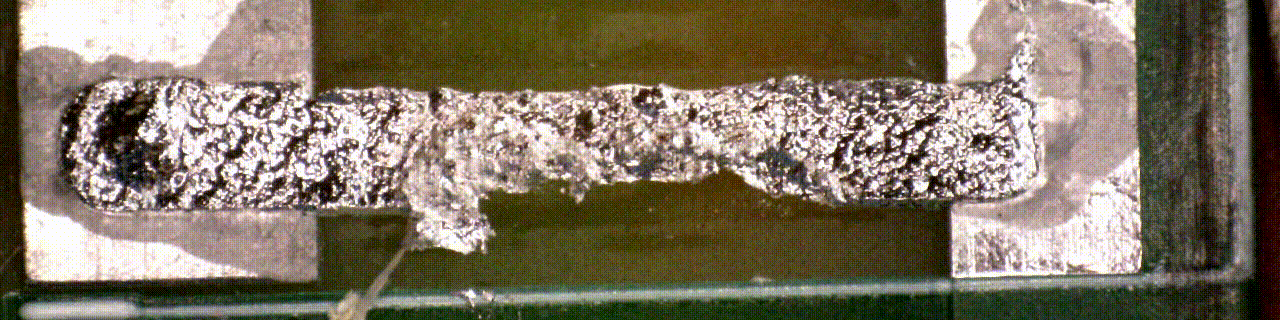
Figure 4. Rapid liquid metal trace degradation under very high current density.
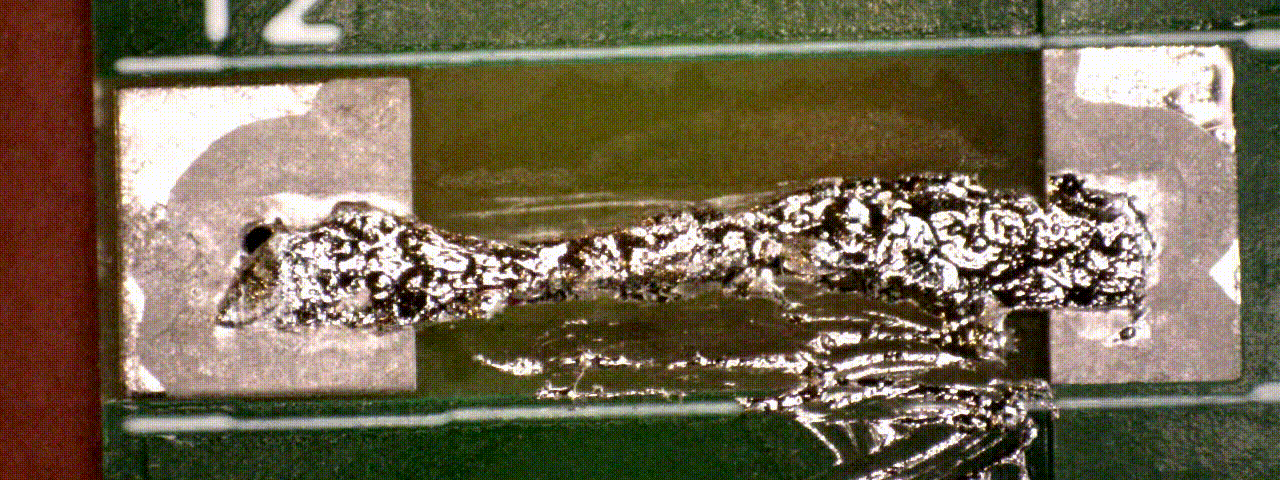
Figure 5. Visual changes due to high current density.
Arieca will continue to push forward on ion migration degradation characterization to better understand how their materials may fail when deployed in applications requiring close proximity to high-voltage supplies, especially in electric vehicles. In this way, they can better understand and help to standardize an approach to evaluating ion migration as a failure mode. These studies can help greatly improve the reliability of materials in safety-critical, high-power electronics, ultimately contributing to the advancement and safety of electric vehicles and other high-voltage applications.